Front-End Semiconductor Solutions
NanoSeeX leads semiconductor innovation worldwide, redefining chip manufacturing with cutting-edge solutions.
Our indigenous high-end equipment and advanced material analysis, coupled with multiphysics models and Al-driven machine learning, drive the forefront of semiconductor technology. Leveraging sub-nanometer X-rays, we achieve unrivaled 0.1 nm resolution, unveiling intricate 3D nanostructures devices. Empowering chipmakers for faster, energy-efficient microchips, we stand as the premier choice for industry partnerships and acquisitions.
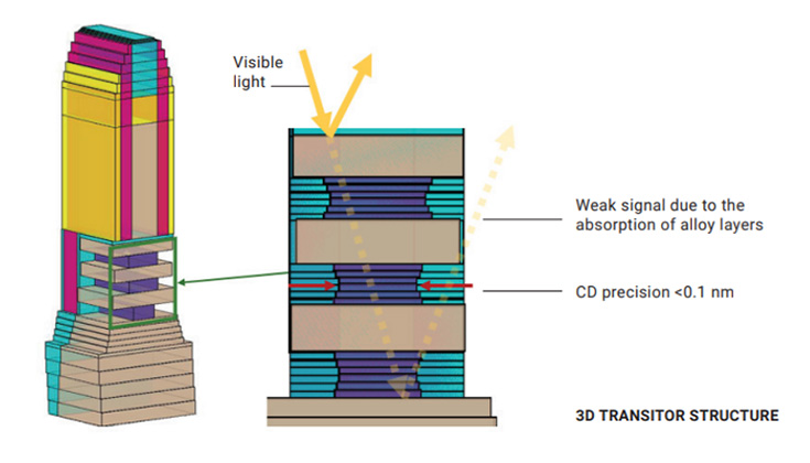
Metrology challenges in advance transistor structure
- Shrinking sizes
- Transition from 2D to complex 3D structures
- Introduction of metal or alloy materials
Navigating Semicon Xcellence
We are spearheading semiconductor innovation, driving the transformation of chip manufacturing processes. With semiconductor processes progressing towards the 2 nm node and beyond, featuring shrinking transistor sizes and a transition from 2D to 3D structures, as well as the integration of metal or alloy materials, the shortcomings of existing optical measurement methods become increasingly evident. As a result, critical dimensions cannot be precisely measured, directly affecting yield and resulting in unfavorable outcomes.